


What Is Transistor?
A transistor is a three-terminal electronic device that regulates the flow of electrical current or amplifies electronic signals. It is typically made of semiconductor materials like Silicon (Si), Germanium (Ge). It consists of three layers or regions: the emitter, the base, and the collector.

Transistors are used in electronic circuits to perform various functions, such as amplification, switching, and voltage regulation. They are a fundamental component in modern electronics and play a vital role in devices like computers, smartphones, televisions, and many other electronic systems.

Table of Contents
Brief history of transistors
The development of the transistor can be attributed to the work of three scientists at Bell Laboratories in the United States: John Bardeen, Walter Brattain, and William Shockley. In 1947, they successfully created the first working transistor.
The invention of the transistor was a significant breakthrough in the field of electronics, as it replaced bulky and power-hungry vacuum tubes that were used for amplification and switching in electronic circuits at that time.
Transistors were much smaller, more reliable, and consumed less power than vacuum tubes. This breakthrough revolutionized the field of electronics and paved the way for the development of modern electronic devices.
Read more on Diodes
- Diode: SYMBOL, TYPES, WORKING, Characteristics & Applications
- POWER DIODE : Structure, Types, Characteristics & Working
- Zener diode
- Zener Diode as a voltage regulator
- PIN Photodiode | It’s working Principle, Construction, VI Characteristics.
- What is Photodiode? Its operations and applications
Parts of a transistor
A transistor consists of several key parts that work together to control the flow of electrical current or amplify electronic signals. The specific parts vary depending onhe type of transistor, but I’ll provide a general overview of the components commonly found in a bipolar junction transistor (BJT):


- Emitter (E): It is left regions in a BJT. It is moderately size. It is heavily doped (highly concentrated with impurities) to emit majority charge carriers (electrons for NPN and holes for PNP transistors) into the base region.
- Base (B): It is the center region between the emitter and the collector. It is thin and relatively lightly doped. It controls the flow of majority charge carriers from the emitter to the collector region by varying the amount of current or voltage applied to it.
- Collector (C): The collector is the third region (Right side) in a BJT. It is relatively large in size and moderately doped. It collects the majority charge carriers (electrons for NPN and holes for PNP) that flow through the base-emitter junction and allows them to exit the transistor.
- Base-emitter junction: This is the junction formed between the base and emitter regions. It acts as a diode, allowing current to flow from the emitter to the base when forward-biased (appropriate voltage applied) and blocking current in the reverse direction.
- Base-collector junction: This is the junction formed between the base and collector regions. It also acts as a diode and helps control the flow of current from the collector to the base region.
These are the fundamental parts of a BJT transistor.
Types of Transistors
There are two main types of transistors: Bipolar junction transistors (BJTs) and Field-effect transistors (FETs):

Bipolar junction transistors (BJTs)
Bipolar junction transistors (BJT) are classified into two types: NPN (negative-positive-negative) and PNP (positive-negative-positive) transistors.
NPN Transistors: In an NPN transistor, one p-type semiconductor material is sandwich between two n-type semiconductor material. In this configuration, the majority charge carriers are electrons. The emitter is doped with a higher concentration of electrons, while the base is lightly doped and the collector is moderately doped. When a small current flows into the base, it controls a larger current flowing from the emitter to the collector. In such a way, the device control the flow of current. NPN transistors are commonly used for amplification and switching purposes.

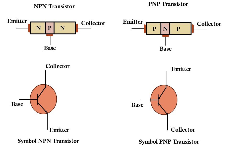
PNP Transistors: In a PNP transistor, one n-type semiconductor material is sandwich between two p-type semiconductor material. In this configuration, the majority charge carriers are holes. The emitter is doped with a higher concentration of holes, while the base is lightly doped and the collector is moderately doped. When a small current flows out of the base, it controls a larger current flowing from the emitter to the collector. PNP transistors also find applications in amplification and switching circuits.
Field-Effect Transistors (FETs):
Field-effect transistors control the flow of current using an electric field. They have three terminals: source, gate, and drain. FETs are further classified into several types, but the two most common are junction field-effect transistors (JFETs) and metal-oxide-semiconductor field-effect transistors (MOSFETs).
Junction Field-Effect Transistors (JFETs): JFETs have a doped semiconductor channel that connects the source and drain regions. The gate terminal controls the width of the channel, which influences the current flow. JFETs can be either N-channel or P-channel, depending on the doping types. They are primarily used for high input impedance applications, such as amplifiers and switches.


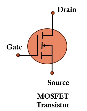
Metal-Oxide-Semiconductor Field-Effect Transistors (MOSFETs): MOSFETs are the most widely used transistors in modern electronics. They have a metal-oxide-semiconductor structure with a gate terminal separated from the channel by an insulating layer (typically silicon dioxide). MOSFETs are further categorized as enhancement-mode (normally off) or depletion-mode (normally on) devices. They offer high input impedance, low power consumption, and excellent switching characteristics. MOSFETs are commonly found in microprocessors, memory devices, and digital circuits.

Transistor Terminals
A transistor has three terminals, each serving a specific function. The names of the terminals may vary slightly depending on the specific transistor type (NPN or PNP for BJTs, or NMOS or PMOS for MOSFETs), but the overall functionality remains the same. Here are the three main terminals of a transistor:
1.Emitter (E) / Source (S):
- In a Bipolar Junction Transistor (BJT), the emitter is the terminal through which majority charge carriers (electrons for NPN and holes for PNP) flow into the transistor.
- In a Field-Effect Transistor (FET), the emitter terminal is referred to as the source terminal.
- The emitter/source terminal is typically marked with an arrow in the transistor symbol.
2. Base (B) / Gate (G):
- The base terminal controls the transistor’s operation. It receives the input signal and controls the flow of charge carriers between the emitter and collector terminals.
- In a BJT, the base terminal is responsible for injecting minority charge carriers (electrons for NPN and holes for PNP) into the base region, allowing or blocking the current flow between the emitter and collector.
- In an FET, the base terminal is known as the gate terminal and controls the conductivity of the channel between the source and drain terminals.
- The base/gate terminal is usually represented by a straight line in the transistor symbol.
3. Collector (C) / Drain (D):
- The collector terminal collects the majority charge carriers (electrons for NPN and holes for PNP) that flow through the transistor.
- In a BJT, the collector terminal is responsible for the majority carrier collection, allowing the transistor to provide amplification or switching capabilities.
- In an FET, the collector terminal is called the drain terminal, and it receives the current from the channel between the source and drain terminals.
- The collector/drain terminal is often represented by an arrow pointing outward from the transistor symbol.
These three terminals work together to control the flow of current through the transistor and enable its amplification or switching behavior. It’s worth noting that the names and symbols for these terminals may vary depending on the transistor type, but their functions remain consistent across different transistor families.
Working Principle of Transistor
There are two main types of transistors: the bipolar junction transistor (BJT) and the field-effect transistor (FET). I’ll provide a brief overview of the operation of each type:
Bipolar Junction Transistor (BJT): The operation of a Bipolar Junction Transistor (BJT) involves the control of current by a small input current at the base terminal.
There are two types of BJTs: NPN and PNP, with slightly different behaviors, but the basic operation principles remain the same. Here’s a detailed explanation of the operation of an NPN BJT:
The BJT operates in three different modes: Active Mode (amplification), Cutoff Mode and Saturation Mode (switching).
- Active Mode: In the active mode, the BJT is used as an amplifier. A small current flows from the base-emitter junction, which controls a much larger current flowing between the collector and emitter. By varying the current at the base-emitter junction, the BJT can amplify or switch electrical signals. Small base current (Ib) controls a much larger collector current (Ic).
- Cutoff Mode: In the cutoff mode, the BJT is effectively switched off, and the collector current is minimal. The base-emitter junction is reverse-biased (Vbe < 0), preventing the flow of base current (Ib) and effectively isolating the collector and emitter regions. Without the flow of base current, there is no amplification, and the collector current (Ic) reduces to a negligible value.
- Saturation Mode: In the saturation mode, the BJT operates as a fully conducting switch. A forward bias voltage (Vbe) is applied to the base-emitter junction, allowing a significant base current (Ib) to flow. The base current enables a large collector current (Ic) to flow freely between the collector and emitter terminals. In this mode, the BJT acts as a closed switch, with minimal voltage drop across the collector-emitter junction.
Field-Effect Transistor (FET): FET transistors are based on the principle of controlling the conductivity of a semiconductor channel using an electric field.
FETs are primarily of two types: the junction field-effect transistor (JFET) and the metal-oxide-semiconductor field-effect transistor (MOSFET).
- In a JFET, a voltage applied between the gate and source terminals creates an electric field that controls the width of the conducting channel between the source and drain terminals.
- In a MOSFET, a thin insulating layer (oxide) separates the gate from the conducting channel, which can be either positively or negatively doped.
- By applying a voltage to the gate terminal, the FET controls the conductivity of the channel, allowing it to amplify or switch electronic signals.
In both types of transistors, the control of current or voltage at one terminal (base/gate) allows the transistor to control or amplify the current or voltage at another terminal (emitter/collector or drain/source). This functionality enables transistors to perform a wide range of functions in electronic circuits, including amplification, signal processing, digital logic, and power regulation.
What is a transistor?
transistor is a three-terminal electronic device that can amplify or switch electronic signals and electrical power. It is a fundamental building block of modern electronic devices and circuits.
What are the main types of transistors?
The two main types of transistors are Bipolar Junction Transistors (BJTs) and Field-Effect Transistors (FETs). BJTs include NPN and PNP transistors, while FETs include Junction Field-Effect Transistors (JFETs) and Metal-Oxide-Semiconductor Field-Effect Transistors (MOSFETs).
What is the difference between an NPN and a PNP transistor?
The main difference lies in the arrangement of the semiconductor layers. In an NPN transistor, the layers are P-N-P, while in a PNP transistor, the layers are N-P-N. The behavior and operation of NPN and PNP transistors are similar, but the polarities of voltages and currents are reversed.
How does a transistor amplify signals?
Transistors amplify signals by controlling a larger current or voltage with a smaller input signal. In the case of a BJT, a small base current controls a much larger collector current. In an FET, a small voltage applied to the gate controls the current flow between the source and drain terminals.
How does a transistor work as a switch?
ransistors can work as switches by operating in either the cutoff or saturation mode. In the cutoff mode, the transistor is switched off, and there is no current flow. In the saturation mode, the transistor is fully conducting, allowing a large current to flow.
What is the difference between a JFET and a MOSFET?
JFETs and MOSFETs are two types of FETs. The main difference is the way the control voltage is applied. In a JFET, a voltage is applied directly between the gate and source terminals. In a MOSFET, a voltage is applied between the gate and source terminals through an insulating layer (oxide).
What are the typical applications of transistors?
Transistors find widespread use in various applications. They are used in amplifiers, audio systems, radios, televisions, computers, digital circuits, power supplies, motor control, and many other electronic devices and systems.
Read more wiki