


If you want to know about what is diode, symbol, formation, Working, types and applications of diode. Please click here


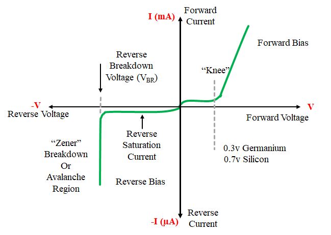
The behavior of a semiconductor diode or p-n junction diode is indicated by its volt-ampere characteristics (V-I characteristics). It is the graph between the voltage across the diode and the current flowing through it.
The Diode symbol and V-I characteristics curve is given below


To make current flow through the diode ,It is necessary to “bias” the diode. So there are two operating regions and three biasing condition for standard diode.
- Zero Bias : No external voltage is applied to the PN junction diode. There is no current flow through it.
- Forward Bias : In forward biased p-n junction diode p-region (anode) connected to positive terminal of the external DC source and n-region (cathode) connected to negative terminal of the external DC source the the biasing is said to be forward biasing .
- Reverse Bias : In reverse biased p-n junction diode p-region (anode) connected to negative terminal of the external DC source and n-region (cathode) connected to positive terminal of the external DC source the the biasing is said to be reverse biasing .
Now according to the biasing the V-I characteristics is divide into two part
- Forward characteristics
- Reverse characteristics
- Forward characteristics of p-n junction Diode : To obtain the forward characteristics of p-n junction diode p-region (anode) connected to positive terminal of the external DC voltage and n-region (cathode) connected to negative terminal of the external DC voltage.


Result the width of the depletion region decreasing and potential barrier also reduces. A very little current, called forward current, flows until the forward voltage exceeds the junction barrier potential (0.3 V for Ge and 0.7 V for Si). Form this instant, the current increases with the increase in forward voltage.
The Forward characteristics is divided into two portion, AB and BC as shown in fig
Region A to B : In region A to B the forward voltage small and less the cut in voltage and the current increases very slowly and the curve is non-linear. Because in this region the external applied voltage to the pn junction is used in overcoming the potential barrier.
Region B to C : As soon as the forward voltage equal to the cut in voltage, current through the diode increases suddenly. The nature of this current is exponential. This large current is limited by connecting a register “R” in series with the diode. The forward is of the order of few mA.
The forward current is a conventional current that flows from anode to cathode. Therefore it is consider as a positive current and the Forward characteristics appears in the first quadrant as shown in fig.
cut-in-voltage (Knee Voltage) : The voltage at which the forward diode current start increasing rapidly know as the “cut-in-voltage” of the diode. The cut-in-voltage is very close to the barrier potential. The cut-in-voltage for silicon diode is 0.7 V and that for germanium diode is 0.3 V.
Reverse characteristics of p-n junction Diode: To obtain the Reverse characteristics of p-n junction diode p-region (anode) connected to negative terminal of the external DC voltage and n-region (cathode) connected to positive terminal of the external DC voltage.


Results in increased depletion region across the junction and potential barrier also increases. Hence the junction resistance becomes very high and no current flow through the diode.
But a very small current flow through the diode called reverse saturation current due to the moment of minority carrier. As the reverse voltage is increased , the reverse saturation current remain constant equal to Io if the temperature is constant. This is because, reverse saturation current does not depend on reverse voltage but it depends only on temperature.
If this reverse applied voltage continuously increases after a certain reverse applied voltage a large reverse current flow through the device & the depletion layer will be destroyed. That reverse voltage is called breakdown voltage (VBR). Result large reverse current flow through the diode.
This large revers current will destroyed the diode. So to protect the diode from this large reverse current a resister “R” is connected in series with the diode. This series resister is called current limiting resister.
Typically reverse breakdown voltage for a p-n junction diode is in the range of 50 to 100 volts.
Hi mam I am new Lerner in basic electronic subject so how to start may jurny in subject plez tell me which concept i am clear step by step
Frist you clear your basics concept of electronics like What is conductors, Insulators, Semiconductors? | Type of semiconductors| Diode etc.
For clear this concepts please refer my you tube video (in English and Hindi both) the link of Basic Electronics playlist is given here: English : https://youtube.com/playlist?list=PLZQgf2pQtimnMYGVCh8k_wsHM0DKqmWp2
Hindi : https://youtube.com/playlist?list=PLZQgf2pQtimn4ls4N2HRTc6qWAbOmD619
Hii ma’am I am Ashish Mahara from Odisha.I need
Power Electronics note and all mcq please provide sequentially….