

Full adder is a combinational logic circuit perform addition of three single bit number. It is a digital circuit has three inputs A, B and Cin , where Cin is the previous carry and two output sum (S), carry (Cout). Here sum is the least significant bit (LSB) and carry is the most significant bit (MSB). Full adder circuit is used in computer ALU (Arithmetic and Logic Unit ) to perform arithmetic operation.
Table of Contents

Truth Table of Full Adder
The full adder circuit perform OR (addition) operation between two single bit binary number A,B and previous carry Cin. Basically, a full adder is a three input and two output combinational circuit. Three inputs A,B and Cin having eight input combinations. After addition of three single bit binary number this circuit produces two outputs Sum (S) and carry (Cout).
Truth table explain the relationship between inputs and outputs.


In the above table,
- A and B are the two single bit inputs and Cin is the previous carry. So, three inputs having 23 = 8 Possible combination.
- When we perform OR operation between three inputs, it produces two output sum (s) and carry (c).
- Here sum is the least significant bit (LSB) and carry is the most significant bit (MSB).
- Carry output is “1” only when the sum of inputs are greater then “1”.
- The least significant bit of the addition is defined by the ‘sum’ bit.
Now, To find the Boolean logical expression from truth table make a k-map for outputs Sum (S) and carry (Cout) and get Boolean expression in SOP form.
If you want to know more on how to design full adder using half adder click here
Know more about Half Adder click here
K-Map for the Sum Output

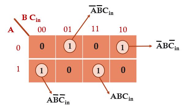
Expression for sum after solving k-map
Sum =A xor B xor Cin
K-Map for Cout

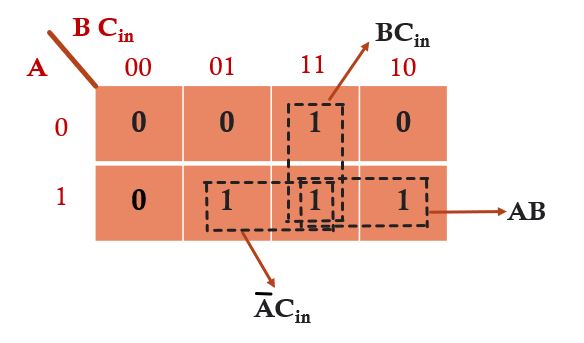
Expression for Cout after solving k-map
Co = AB + ACin +BCin
Now draw the logic diagram of Full adder
A Logic Diagram For Full Adder


For more detail watch my video
Q1: What is a full adder?
A full adder is a combinational logic circuit that adds three input bits: A, B, and a carry input (C_in). It produces a sum (S) output and a carry output (C_out). The carry input (C_in) represents the carry bit from the previous stage of addition.
Q2: How does a full adder differ from a half adder?
While a half adder adds two input bits, a full adder takes into account an additional carry input. This allows the full adder to handle the carry bit from the previous stage, enabling the addition of multiple bits in cascaded adders.
Q3: What is the truth table of a full adder?
The truth table for a full adder consists of the input bits (A, B, C_in) and the corresponding outputs (S, C_out). The table defines all possible input combinations and their resulting outputs.
Q4: What is the circuit diagram of a full adder?
A full adder can be implemented using logic gates such as XOR, AND, and OR gates. The circuit diagram typically includes two XOR gates, two AND gates, and an OR gate, along with the input and output connections.
Q5: How can I cascade multiple full adders to create larger adders?
Multiple full adders can be cascaded by connecting the carry output (C_out) of one full adder to the carry input (C_in) of the next full adder. This allows for the addition of multiple bits, creating n-bit adders.
Q6: What are the practical applications of full adders?
Full adders are fundamental building blocks used in various digital systems. They find applications in arithmetic operations, microprocessors, calculators, memory addressing, and digital signal processing. Full adders are crucial for binary addition and are extensively used in data processing and arithmetic units.
Q7: Can a full adder be implemented using other logic gates?
Yes, a full adder can be implemented using different combinations of logic gates. While the traditional implementation involves XOR, AND, and OR gates, other gate combinations, such as NAND or NOR gates, can also be used to achieve the same functionality.
Q8: What are the considerations for signal propagation and timing?
Propagation delay, signal integrity, and timing are important considerations when working with full adders. Propagation delay refers to the time it takes for signals to propagate through the circuit. Signal integrity ensures accurate and reliable data transmission. Timing considerations involve meeting setup and hold time requirements to avoid timing violations.
Wiki link for adder here