

Definition
“A Schottky Diode is a metal-semiconductor diode with a low forward voltage drop and a very fast switching speed”
What Is Schottky Diode ?
The Schottky Diode is another type of semiconductor diode but have the advantage that their forward voltage drop is less (0.15 to 0.3V) than that of the conventional silicon pn-junction diode (0.6 to 0.7V). Schottky diode is also known as Schottky barrier diode, surface barrier diode, majority carrier device, hot-electron diode, or hot carrier diode.
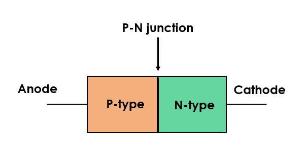
In a conventional P-N junction diode, a P-type semiconductor and an N-type semiconductor are used to form the P-N junction. When a P-type semiconductor is joined with an N-type semiconductor, a junction is formed known as P-N junction.
Where as Schottky diode is a metal-semiconductor diode. When a metals (such as aluminum, platinum, gold, tungsten) and N-type semiconductor is joined, a junction is formed between metal and N-type semiconductor. This junction is known as a M-S junction or metal-semiconductor junction. A metal-semiconductor junction formed creates a barrier or depletion layer known as a Schottky barrier.
Schottky diode is a unipolar device because in Schottky diode both the metal and n-type semiconductor have electrons as their majority carriers, as almost negligible holes are present in a metal. i.e., electrons are responsible for conduction. Hence it is a unipolar device.
Where as normal p-n junction diode is a bipolar device because in normal p-n junction diode p-type semiconductor have majority carrier holes and n-type semiconductor have majority carrier electrons. So here both electrons and holes are responsible for conduction. Hence it is called bipolar device.


The Schottky diode is named after German physicist Walter H. Schottky.
Schottky diode can switch on and off much faster than the normal p-n junction diode. Also, the Schottky diode produces less unwanted noise than normal p-n junction diode. These two characteristics of the Schottky diode make it very useful in high-speed switching applications.


Just like a conventional P-N junction diode, a Schottky diode will conduct a current in the forward direction when sufficient forward voltage is applied. But a silicon PN junction diode has a typical forward voltage of 0.6–0.7 Volts, while Schottky’s forward voltage is 0.2–0.3 Volts.
Symbol of Schottky Diode
The symbol of the Schottky diode is shown in the figure below.
Here, the anode is the metal side and the cathode is the semiconductor side.


Construction Of Schottky Diode
Schottky Diode are formed by joining n-type semiconductor substrate and a metal. This metal and semiconductor junction is called M-S Junction. The metal used for fabrication of Schottky diode can be gold, tungsten, platinum silver etc . This M-S junction creates a barrier or depletion layer known as a Schottky barrier.


Two types of Schottky barriers are formed near the junctions these are Rectifying and Non-rectifying type. When a metal is joined with lightly doped n-type semiconductor this is called non-ohmic contact. In non-ohmic contact a large depletion region is formed near the junction this will create large Schottky barrier across the junction and this Schottky barrier is called rectifying Schottky barrier. Sequentially When a metal is joined with heavily doped n-type semiconductor this is called ohmic contact. In ohmic contact a thin or negligible depletion region is formed near the junction this will create small Schottky barrier across the junction and this Schottky barrier is called non-rectifying Schottky barrier.
So we can say that, the non-rectifying metal-semiconductor junction or ohmic contact offers very low resistance to the electric current whereas the rectifying metal-semiconductor junction or non-ohmic contact offers high resistance to the electric current as compared to the ohmic contact.
Working of Schottky Diode
Unbiased Schottky diode
When the metal is combined with the n-type semiconductor , the free electrons in the n-type semiconductor will move from n-type semiconductor to metal. Device will reached to its equilibrium state. When free electrons moves across the junction, it provides an extra electron to the atoms present in the metal. Due to this, atoms present in the metal junction receive an extra electron and become negative ions.

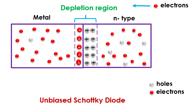
The atoms at n-side junction lose electrons and become positive ions. Thus, positive ions collected near the n-side junction and negative ions collected near the metal junction. These positive and negative ions create a depletion region near the junction. The width of the depletion region is is negligibly thin in metal as compare to n-type semiconductor. This depletion region will create a potential barrier near the junction, and this potential barrier is called Schottky barrier. This barrier stopped the movement of electron across the junction.
To overcome this barrier, the free electrons need energy greater than the built-in-potential across the junction.
Forward biased Schottky diode
In forward biased metal is connected with positive terminal of battery and n-type is connected with negative terminal of battery. When forward bias voltage is applied, a large number of free electrons are generated in the metal and n-type semiconductor. If the applied forward biased voltage is less than the built-in-potential (i.e. 0.2 volts ) across the junction, no free electrons in n-type semiconductor and metal move cross the junction.

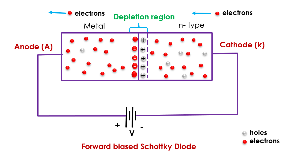
If the applied voltage is greater than built-in-potential (i.e. 0.2 volts ) , the free electrons gain enough energy and overcomes the built-in-potential of the depletion region. Due to this , electric current starts flowing through the Schottky diode.
So Schottky diode have low forward turn on voltage (0.2 to 0.3 Volts) as compare to normal p-n junction diode forward turn on voltage (0.3 to 0.7 volts).
This lower forward voltage requirement enables Schottky diodes to have higher switching speeds and increased efficiency.
Reverse biased Schottky diode
In Reverse biased metal is connected with negative terminal of battery and n-type is connected with positive terminal of battery.

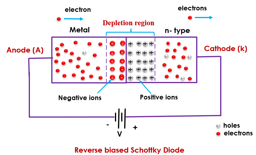
When reverse bias voltage is applied, a large depletion region grow across the junction. Due to this, large potential barrier developed across the junction. As a result, the electric current stops flowing the device. However, a small reverse leakage current flows through the device due to the thermally excited electrons in the metal.
When further in increased in reverse bias voltage, the depletion region become weaker and current start increasing gradually. If high reverse bias voltage is applied the junction will be breakdown and suddenly large revers current flow across the device. Which may permanently damage the device.
V-I Characteristics of Schottky diode
The V-I characteristics of Schottky diode is shown figure below. The V-I characteristics of Schottky diode is almost similar to the P-N junction diode. The forward voltage drop of Schottky diode is very low (0.2 to 0.3 volts) as compared to the normal P-N junction diode (0.6 to 0.7 volts).
The turn-on voltage for a Schottky diode is very low as compared to the p-n junction diode. If the forward bias voltage is higher than 0.2 or 0.3 volts, electric current starts flowing through the Schottky diode.
In Schottky diode, the reverse saturation current occurs at a very low reverse bias voltage as compared to the silicon p-n junction diode.
Features Of Schottky Diode:
- Higher efficiency
- Low forward voltage drop
- Low capacitance
- Low profile surface-mount package, ultra-small
- Integrated guard ring for stress protection
Difference between Schottky diode and normal p-n junction diode
- Schottky diode is a unipolar device because in Schottky diode both the metal and n-type semiconductor have majority carriers electrons. Here, electrons are responsible for conduction. Where as normal p-n junction diode is a bipolar device because in normal p-n junction diode p-type semiconductor have majority carrier holes and n-type semiconductor have majority carrier electrons. So here both electrons and holes are responsible for conduction.
- The depletion region is negligible or absent in case of Schottky diode, whereas in p-n junction diode the depletion region is present.
- Schottky diode reverse breakdown voltage is very small as compared to the normal p-n junction diode.
- The forward voltage drop of Schottky diode is very less as compared to normal p-n junction diode.
- The switching Speed of Schottky diode is higher than normal p-n junction diode. Because the forward on state voltage drop of Schottky diode is low as compare to normal p-n junction diode.
Applications of Schottky diodes
- Schottky diode Used in radio frequency (RF) applications.
- Schottky diode Used in Switched-mode power supplies (SMPS).
- Schottky diode Used in various protection circuits.
- Schottky diode Used in voltage clamping application.
- Schottky diode Used in RF mixer and Detector diode.
- Schottky diode Used in solar cell application.
- Schottky diode used in logic circuits (like TTL and CMOS logic circuits).
Frequently Asked Questions
A Schottky Diode is a metal-semiconductor diode with a low forward voltage drop than the P-N junction diode and a very fast switching speed.
when electrons are energized then jumped over a metal which is has high energy state. Due to this high energy metal involvement it is called hot carrier diode.
According to definition, device using both majority and minority charge carriers are called minority carrier device. For example, PN diode uses both holes and electrons as charge carrier.
Device using only one type of charge carriers is called Majority Carrier Device. Fire example, Schottky diode which uses only electrons as charge Carrier.
Schottky diode Used in radio frequency (RF) applications.
Schottky diode Used in Switched-mode power supplies (SMPS).
Schottky diode Used in various protection circuits.
Schottky diode Used in voltage clamping application.
Schottky diode Used in RF mixer and Detector diode.
Schottky diode Used in solar cell application.
Schottky diode used in logic circuits (like TTL and CMOS logic circuits).
Best note for ECE student
Thanks ma’am.
Would a Schottky diode be considered integrating, proportional, or differentiating? I must be over thinking this question…