
SINGLE-PHASE BRIDGE-TYPE INVERTERS
We know that, in case of parallel inverter has disadvantages that it uses heavy transformer to carry the load current. Also, in the parallel capacitor inverter large amount of energy is trapped in the commutating capacitor which is need to be removed with additional circuit components. These disadvantages are overcome by using bridge-type inverter which eliminates the need of the magnetic components such as the center-tap transformer or large capacitor. Only semiconductor components are used in this type of inverter.
Single Phase Half Bridge Inverter RL load
This type of inverter is very simple in construction. It is a half bridge inverter circuit consist of two thyristors T1 & T2 and two feedback diode D1 & D2, each diode is connected in anti-parallel with each thyristor and three wire DC source that provide balance DC voltage at source.
The basic configuration of this inverter is shown in figure.


In single phase inverter instead of thyristor here we use any other power semiconductor switching device like IGBT, Power MOSFET etc.
Here assumed that, each thyristor conducts for the duration its gate signa is present and is commutated when this signal is removed. The gating signal for thyristor T1 and thyristor T2 are ig1 and ig2 respectively.
Load RL is connected between point A and B. Point A is always considered as +ve w.r.t point B. If the current flow in this direction we assume that current is +ve.
Similarly, if current from B to A the current is considered -ve.
Due to inductive load the output voltage waveform is just similar to that of R-load. However, the output current wave form is not similar to the output voltage waveform.
In case of RL load the output, current Io is the exponential function of time and output current lag output voltage by an angle ϕ.
Φ = tan-1 (ωL/R)
Operation of Single-Phase Half Bridge Inverter with RL- Load
The operation of Half Bridge Inverter is divided into four modes.
- Mode I: (t1< t < T/2) T1 on
- Mode II: (T/2 < t < t2) D2 on
- Mode III: (t2 < t < T) T on
- Mode IV: (0 < t < t1) D1, D2 on
Mode I (t1< t < T/2):
In this duration, we give gate pulse to thyristor T1. So T1 get turned on at time instant t1 and current flow from the upper half of supply voltage and current follow the path Vs/2 (Upper Supply) ….. T1 ….. load ….. back to Vs/2. In this mode inductor store energy and output current increases exponentially as a function of time from zero to its positive max value (Imax). and induced voltage across inductor +VL– .

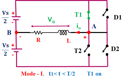
This time output voltage is also positive because point A is positive (+ve) w.r.t point B.
Applying KVL,
Vs/2 – V0=0
The magnitude of output voltage Vo = Vs/2.
At time instant T/2 the output current reaches to its maximum value and thyristor T1 will be off at this time instant due to the same polarity of voltage and current.
Mode II (T/2 < t < t2):
After time instant T/2 inductor dissipated energy and we know that when inductor dissipated energy it changes its polarity. And we know that the property of inductor, inductor can’t allow sudden change in current. So, inductor slowly release its energy through the D2 diode. D2 diode is conduct this time and current follow the path, Load ….. lower half of supply (Vs/2) …… D2 ….. back to Load at this time interval the energy release by inductor feedback to the lower half supply.

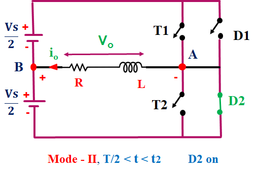
At this mode output current is positive but gradually decreases from Imax to zero because of energy dissipated by the inductive load. The Output voltage is negative (-Vs/2) this time because point B is positive w.r.t. A.
Mode III (t2 < t < T):
At time instant t2, thyristor T2 get turned on and current flow in a lower half of the circuit and follow the path Vs/2 (lower supply) …. load …..T2…. back to Vs/2. So, the direction of current is reverse because point B is positive w.r.t. A and inductor store energy in reverse direction from (-Imax) to zero.

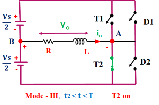
At this time output voltage across load is negative (-Vs/2).
Mode IV (0 < t < t1):
This time interval operation is just similar to time interval after T. In this duration, D1 is on.

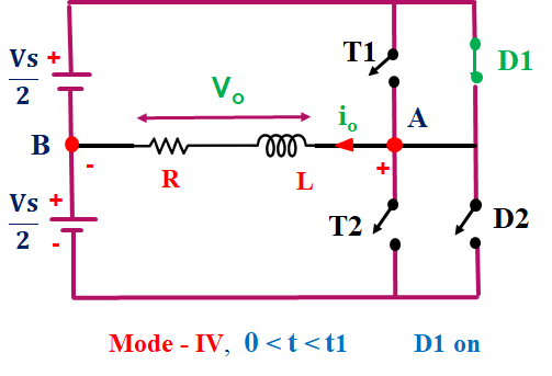
At time instant T the output voltage and output current having same polarity. Therefore, T2 is turned off due to inductive load and D1 turned on. And current flow from load …. D1…. Vs/2 (Upper supply) …. back to the load.
Here energy release by the inductor fad back to the upper part of supply voltage Vs/2. This time point A is positive w.r.t point B. So, output voltage is positive Vs/2 and output current decreases exponentially from its negative max value (-Imax) to zero.
Now Draw the waveform for Single Phase Full Bridge VSI (RL Load)

