


8086 was the first 16-bit microprocessor available in 40-pin DIP (Dual Inline Package) chip. Let us now discuss in detail the pin configuration of a 8086 Microprocessor.


Hindi Video

English Video

Table of Contents
Introduction of 8086 Microprocessor
- Intel 8086 was the first 16-bit HMOS microprocessor.
- All the limitation of 8-bit microprocessor is overcome by 16-bit microprocessor.
- It is a more powerful processor in term of advanced architecture, more processing capability, large memory addressing capability and more powerful instruction set.
- It is available in 40 pin DIP chip (40 pin IC).
- It uses a +5V DC supply for its operation.
- The 8086 uses 20-line address bus. It has a 16-bit data bus.
- The 20 line of the address bus operate in multiplexed mode. The 16-low order address bus lines have been multiplexed with data and 4 high-order address bus lines have been multiplexed with status signals.
More read on microprocess
Difference between Microprocessor and Microcontroller
All video related to 8086 Microprocessor
8086 Pin Diagram
8086 was the first 16-bit microprocessor available in 40-pin DIP (Dual Inline Package) chip. Let us now discuss in detail the pin configuration of a 8086 Microprocessor.

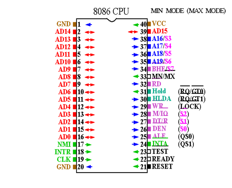
A16/S3, A17/S4, A18/S5, A19/S6 : High order address bus. These are multiplexed with status signals. These lines are high for memory related operation and low for I/O related operation. These are multiplexed with status signal S3 to S4 respectively. The combination of S3 ,S4 determine that which part of memory is to be accessed. Where S6 is always low logic and reserved for future use. S5 for interrupt status
| A17/S4 | A16/S3 | FUNCTION |
| 0 | 0 | Extra segment access |
| 0 | 1 | Stack segment access |
| 1 | 0 | Code segment access |
| 1 | 1 | Data segment access |
•BHE/S7 : BHE signal is enable when data bit are 16 bit it transfer of data over higher order data bus. If it is 1 then data is less than 8 bit.


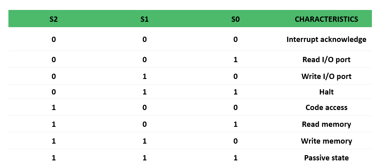
S2, S1, S0 : Status pins. All are active low pin. These are used by the 8288 bus controller for generating all the memory and I/O operation access control signals. Any change in S2, S1, S0 indicates the beginning of a bus cycle

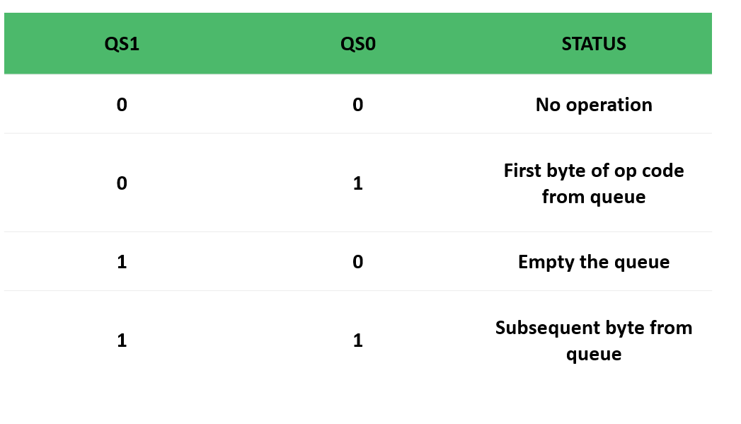
•QS1,QS0 : Queue Status. These signals indicate the status of the internal 8086 instruction queue according to the table shown below

Power supply and frequency signals
It uses 5V DC supply at VCC pin 40, and uses ground at VSS pin 1 and 20 for its operation.
Clock signal
Clock signal is provided through Pin-19. It provides timing to the processor for operations. Its frequency is different for different versions, i.e. 5MHz, 8MHz and 10MHz.
Address/data bus
AD0-AD15. These are 16 address/data bus. AD0-AD7 carries low order byte data and AD8AD15 carries higher order byte data. During the first clock cycle, it carries 16-bit address and after that it carries 16-bit data.
Address/status bus
A16-A19/S3-S6. These are the 4 address/status buses. During the first clock cycle, it carries 4-bit address and later it carries status signals.
S7/BHE
BHE stands for Bus High Enable. It is available at pin 34 and used to indicate the transfer of data using data bus D8-D15. This signal is low during the first clock cycle, thereafter it is active.
Read($\overline{RD}$)
It is available at pin 32 and is used to read signal for Read operation.
Ready
It is available at pin 22. It is an acknowledgement signal from I/O devices that data is transferred. It is an active high signal. When it is high, it indicates that the device is ready to transfer data. When it is low, it indicates wait state.
RESET
It is available at pin 21 and is used to restart the execution. It causes the processor to immediately terminate its present activity. This signal is active high for the first 4 clock cycles to RESET the microprocessor.
INTR
It is available at pin 18. It is an interrupt request signal, which is sampled during the last clock cycle of each instruction to determine if the processor considered this as an interrupt or not.
NMI
It stands for non-maskable interrupt and is available at pin 17. It is an edge triggered input, which causes an interrupt request to the microprocessor.
$\overline{TEST}$
This signal is like wait state and is available at pin 23. When this signal is high, then the processor has to wait for IDLE state, else the execution continues.
MN/MX
It stands for Minimum/Maximum and is available at pin 33. It indicates what mode the processor is to operate in; when it is high, it works in the minimum mode and vice-versa.
INTA
It is an interrupt acknowledgement signal and id available at pin 24. When the microprocessor receives this signal, it acknowledges the interrupt.
ALE
It stands for address enable latch and is available at pin 25. A positive pulse is generated each time the processor begins any operation. This signal indicates the availability of a valid address on the address/data lines.
DEN
It stands for Data Enable and is available at pin 26. It is used to enable Transreceiver 8286. The transreceiver is a device used to separate data from the address/data bus.
DT/R
It stands for Data Transmit/Receive signal and is available at pin 27. It decides the direction of data flow through the transreceiver. When it is high, data is transmitted out and vice-versa.
M/IO
This signal is used to distinguish between memory and I/O operations. When it is high, it indicates I/O operation and when it is low indicates the memory operation. It is available at pin 28.
WR
It stands for write signal and is available at pin 29. It is used to write the data into the memory or the output device depending on the status of M/IO signal.
HLDA
It stands for Hold Acknowledgement signal and is available at pin 30. This signal acknowledges the HOLD signal.
HOLD
This signal indicates to the processor that external devices are requesting to access the address/data buses. It is available at pin 31.
LOCK
When this signal is active, it indicates to the other processors not to ask the CPU to leave the system bus. It is activated using the LOCK prefix on any instruction and is available at pin 29.
RQ/GT1 and RQ/GT0
These are the Request/Grant signals used by the other processors requesting the CPU to release the system bus. When the signal is received by CPU, then it sends acknowledgment. RQ/GT0 has a higher priority than RQ/GT1.
FAQ
Q: What is the 8086 microprocessor?
The 8086 microprocessor is a 16-bit microprocessor chip developed by Intel in the late 1970s. It was the first member of the x86 processor family and marked a significant milestone in the history of personal computers.
Q: When was the 8086 microprocessor released?
The 8086 microprocessor was released by Intel in 1978.
What is the architecture of the 8086 microprocessor?
The 8086 microprocessor follows the complex instruction set computer (CISC) architecture. It has a 16-bit data bus, a 20-bit address bus, and supports a wide range of instructions.
What are the key features of the 8086 microprocessor?
The key features of the 8086 microprocessor include its 16-bit architecture, segmented memory model, support for 1 megabyte of memory, instruction pipelining, and a rich set of instructions.
Q: What is the difference between the 8086 and 8088 microprocessors?
The 8086 and 8088 microprocessors are very similar, but the main difference lies in the external data bus width. The 8086 has a 16-bit data bus, while the 8088 has an 8-bit data bus. This difference affected the performance and cost of systems using these processors.
Q: What is the maximum memory capacity supported by the 8086 microprocessor?
The 8086 microprocessor can address up to 1 megabyte (2^20 bytes) of memory. However, due to its segmented memory model, it requires additional programming techniques to fully utilize the entire memory space efficiently.
Q: What is the segmented memory model in the 8086 microprocessor?
The segmented memory model in the 8086 microprocessor divides the memory into multiple segments of up to 64 kilobytes each. It uses a 16-bit segment register and a 16-bit offset to form a 20-bit physical address, allowing access to a total of 1 megabyte of memory.
Q: What is instruction pipelining in the 8086 microprocessor?
Instruction pipelining is a technique used in the 8086 microprocessor to improve instruction execution speed. It divides the execution of instructions into multiple stages, allowing multiple instructions to be processed simultaneously. This overlapping of instruction execution stages improves overall performance.
Q: What operating systems were compatible with the 8086 microprocessor?
The 8086 microprocessor was compatible with various operating systems, including MS-DOS (Microsoft Disk Operating System), PC DOS, and early versions of Windows. It also served as the foundation for the x86 architecture, which is still widely used today.
Q: What is the legacy of the 8086 microprocessor?
The 8086 microprocessor played a crucial role in the development of personal computers. Its architecture served as the foundation for the x86 processor family, which has evolved over the years and continues to dominate the market. Many modern software applications and operating systems are designed to run on x86-based systems, ensuring the lasting impact of the 8086 microprocessor.
Wiki link