


Please check video lecture on what is Diode, symbol, working and Its applications

What is Diode ?
Diode is a two electrode or two terminal electronics device, that conducts current only in one direction. So we can say that diode is a unidirectional device which allows the flow of current in only one direction while blocks the flow of current in opposite or reverse direction. It is work like a switch.
An ideal diode act as a perfect conductor with zero resistance in forward direction and act as a perfect insulator with infinite resistance in reverse direction. But Practically no diodes can be act as a ideal diode, always they offer a low resistance in forward direction and very high resistance in the reverse direction.
The most common type of diode is P-n Junction semiconductor diode. The diode is made either of the two semiconductor materials, silicon or germanium. For designing the diodes, silicon is more preferred over germanium because silicon semiconductors diode works at higher temperature compared with germanium diode.
Diode having two terminal anode and cathode. Diode is said to be “forward biased” when anode is positive w.r.t. cathode, So current flow in forward direction. So we can say that diode is in conducting state (offer low resistance forward direction). Diode is said to be “Reverse biased” when cathode is positive w.r.t. anode, So no current flow in reverse direction. So we can say that diode is in non-conducting state (offer high resistance reverse direction).
Symbol Of Diode
The symbol of diode is given below, a triangle adjoining the line. The arrowhead in the symbol points the direction of electric current flow through the device . Diode having two terminal anode and cathode. The anode terminal is connected to the p side and the cathode terminal is connected to the n side.


Formation of Diode
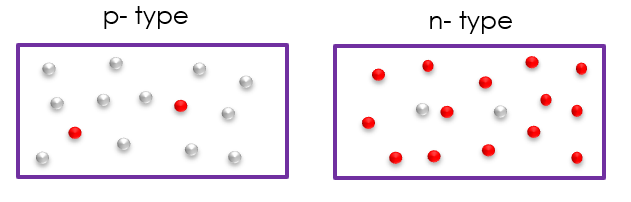
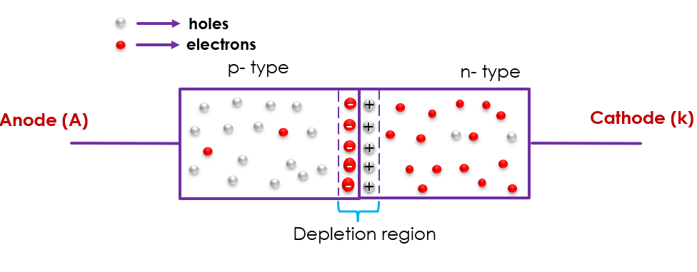
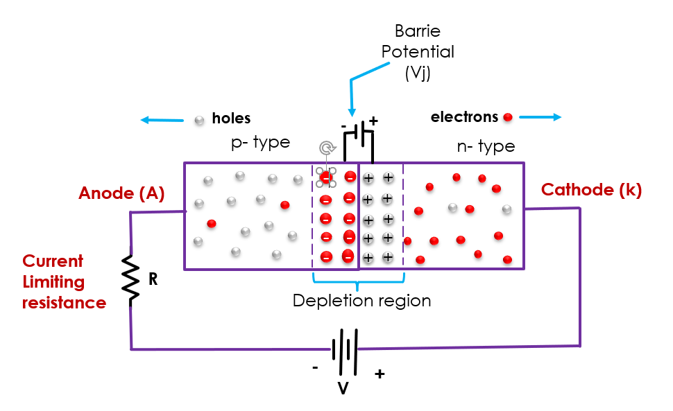
To create a simple p-n junction diode we take a n-type semiconductor and a p-type semiconductor material. In n-type semiconductors, free electrons are the majority charge carriers where as in p-type semiconductors, holes are the majority charge carriers. When the n-type semiconductor is joined with the p-type semiconductor, a p-n junction is formed. And a depletion layer is formed near the junction. The width of depletion layer is depend on the doping level of semiconductor material. Depletion layer is thick in lightly doped semiconductor material and thin in heavy doped semiconductor material. The terminal connected to the p-type is the anode. The terminal connected to the n-type side is the cathode.


Biasing of Diode
To make the current to flow through the diode, It is necessary to “bias” the diode. “The process of applying the external DC voltage to a p-n junction semiconductor diode is called biasing”.
- Zero Biased Diode
- Forward Biased Diode
- Reverse Biased Diode
Zero Biased Diode (Unbiased Diode)
Zero biased p-n junction diode means when no external DC voltage applied to the terminals.
Now let as see what happen when no external DC voltage applied to the terminals. To create a simple p-n junction diode we take a n-type semiconductor and a p-type semiconductor material. In n-type semiconductors, free electrons are the majority charge carriers where as in p-type semiconductors, holes are the majority charge carriers.
When the n-type semiconductor is joined with the p-type semiconductor, a p-n junction is formed. And a depletion layer is formed near the junction due to concentration gradient. Now due to concentration differences, majority carriers diffuse from one side to another.
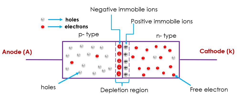
As the concentration of holes is high in the p-type region and it is low in the n-type region, the holes start diffusing from the p-type region to the n-type region. In the Same way, as the concentration of electrons is high in the n-type region and it is low in the p-type region, the electron start diffusing from the n-type region to the p-type region and recombine with holes available there. Each electron diffusing into the “p” side will leave behind a positive immobile ion on the n-side.
When an electron combine with a hole on the “p” side, an atom which accepts this electron, loses its electrically neutral status and becomes a negative immobile ion. Due to tis recombination process, large number of positive immobile ion accumulate near the junction on the n-side and large number of negative immobile ion accumulate near the junction on the p-side.
The negative charged ion on the p-side will start repelling the electrons which attempt to diffuse into p-side and after some time diffusion will be stop completely . At this point junction is said to be in equilibrium state.

Forward Biased Diode
In forward biased p-n junction diode p-region (anode) connected to positive terminal of the external DC source and n-region (cathode) connected to negative terminal of the external DC source the the biasing is said to be forward biasing .

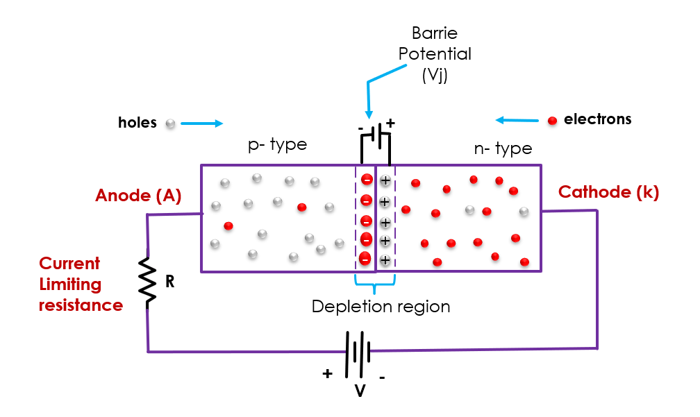
Due to the negative terminal of external source connected to the n- region, free electrons from n- side are pushed towards the p- side. Similarly the positive end of the supply will push holes from p- side toward the n- side.
With increasing in the external supply V , large number of holes (p-side) and electrons (n-side) start travelling towards the junction. As the result of this, the width of depletion region will reduce. Due to reduction in the depletion region barrier potential also reduce. And a particular value of supply voltage depletion region will collapse. Hence large number of majority carrier (electrons and holes) can cross the junction and large current will flow that current is called forward current from anode to cathode.
Reverse Biased Diode
In reverse biased p-n junction diode p-region (anode) connected to negative terminal of the external DC source and n-region (cathode) connected to positive terminal of the external DC source the the biasing is said to be reverse biasing .

Due to the reverse biased, holes in the p-region are attracted toward negative terminal of supply and move away from the junction. Similarly electron in the n -region are attracted toward positive terminal of supply and move away from the junction.
Due to this moment of electron and hole away from the junction the width of the depletion region increases and barrier potential will also increased resulting no current flow through the device. But a small current flow through the diode called reverse saturation current due to the moment of minority carrier. If this reverse applied voltage continuously increases after a certain reverse applied voltage a large revers current flow through the device & the depletion layer will be destroyed. The external voltage at which the the depletion layer will be completely destroyed that voltage is called Revers Breakdown Voltage. When junction breakdown take place large reverse current flow across the device. If this revers current not limited by a external resistance it will destroyed the diode.
Applications of Diode
The various applications of diodes are :-
- Diode is work like a switch : A p-n junction diode is used as electronic switch in digital logic circuits.
- Diode also work as a Rectifier : A p-n junction diode can be used to convert the alternating current (AC) to the direct current (DC).
- Diodes in Logic Gates: Diode also use in many digital logic gates to perform logic operations.
- Diodes in Clamping Circuits: A clamper circuit is used to shift or alter either positive or negative peak of an input signal to a desired level. This circuit is also called as level shifter or DC restorer. These clamping circuits can be positive or negative depends on the diode configuration.
- Diodes in Clipping Circuits: The clipper circuit is used to put off the voltage beyond the preset value without disturbing the remaining part of the input waveform. Based on the diode configuration in the circuit, these clippers are divided into two types; series and shunt clipper.
Types Of Diode
- Light Emitting Diode (LED)
- P-N junction diode
- Zener diode
- Schottky diode
- Avalanche diode
- Photodiode
- Laser diode
- PIN diode
- Varactor diode
- Tunnel diode