

Half adder is a combinational logic circuit perform addition of two single bit number. It is a digital circuit has two input X, Y and two output sum (S), carry (C). Here sum is the least significant bit (LSB) and carry is the most significant bit (MSB). Half adder circuit is used in computer ALU (Arithmetic and Logic Unit ) to perform arithmetic operation.

Table of Contents


Truth Table of Half Adder
The half adder circuit perform OR (addition) operation between two single bit binary number. Two input X and Y having four input combination. After addition of two single bit binary number this circuit produces two outputs Sum (S) and carry (C).
Truth Table
Truth table explain the relationship between inputs and outputs.


In the above table,
- X and Y are the two inputs and two input having 22 = 4 Possible combination.
- When we perform OR operation between two inputs, it produces two output sum (s) and carry (c).
- Here sum is the least significant bit (LSB) and carry is the most significant bit (MSB).
- Carry output is “1” only when both the inputs are “1”.
- The least significant bit of the sum is defined by the ‘sum’ bit.
Now, we find the Boolean logical expression from truth table for outputs Sum (S) and carry (C) in SOP form.
Now , we draw the circuit diagram using logical expression of Sum (S) and Carry (C)
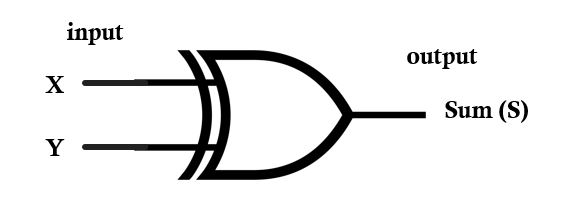
Sum = X’Y+XY’ = X xor Y
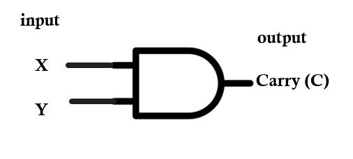
Carry = XY
Sum bit is generated with the help of the Exclusive-OR or XOR Gate
Sum = X’Y+XY’ = X xor Y

Carry bit is generated with the help of the AND Gate
Carry = XY

Now, add above sum and Carry circuits to get half adder circuit diagram

Full Adder read here
Full Adder using half adder read here
FAQ
Q1: What is a half adder?


A half adder is a basic digital circuit that performs the addition of two single-bit binary numbers. It has two inputs, A and B, and two outputs, the sum (S) and the carry (C). The half adder does not consider any carry input from previous stages.
Q2: What is the truth table of a half adder?
The truth table for a half adder consists of the input bits A and B and the corresponding outputs S (sum) and C (carry). The table defines all possible input combinations and their resulting outputs.
Q3: How is a half adder implemented?
A half adder can be implemented using basic logic gates such as XOR (exclusive OR) and AND gates. The XOR gate computes the sum output, while the AND gate generates the carry output.
Q4: What are the limitations of a half adder?
A half adder can only perform the addition of two input bits and does not account for any carry input. Therefore, it cannot handle multi-bit additions or propagate carry bits from previous stages of addition.
Q5: Can half adders be cascaded to perform multi-bit additions?
No, half adders alone cannot be cascaded to perform multi-bit additions. To add multi-bit numbers, full adders are used, which incorporate carry inputs from previous stages.
Q6: What are the practical applications of a half adder?
While a half adder may not be sufficient for complex arithmetic operations, it serves as a building block for larger adders and other digital circuits. It is often used in the design of arithmetic logic units (ALUs), counters, and various other combinational logic circuits.
Q8: Can a half adder be implemented using different logic gates?
Yes, a half adder can be implemented using different combinations of logic gates. While the traditional implementation involves XOR and AND gates, other gate combinations, such as NAND or NOR gates, can also be used to achieve the same functionality.
wiki link