


What Is PIN Diode?
A PIN photodiode is a specialized semiconductor device that converts light energy into an electrical current.


It is widely used in various applications, ranging from optical communications and sensing to medical imaging and scientific research.
The unique structure and operating principle of a PIN photodiode make it a versatile and efficient light detector.
Read more about Photo Diode click here
Table of Contents
Characteristics Of PIN Photodiode
- Reverse Bias Operation:
- PIN photodiodes are typically operated under reverse bias voltage, meaning the P-side is connected to the positive terminal and the N-side to the negative terminal.
- The reverse bias voltage increases the width of the depletion region, enhancing the light absorption capability of the photodiode.
- 2. Fast Response Time:
- PIN photodiodes have a fast response time, allowing them to detect and respond to light signals quickly.
- The fast response time is crucial for applications that require the detection or modulation of high-frequency light signals.
- High Sensitivity:
- PIN photodiodes are highly sensitive to light, enabling them to detect even low-level light signals or weak light intensities.
- This high sensitivity makes them suitable for applications that require accurate detection in low-light conditions or demanding environments.
- Low Noise:
- PIN photodiodes exhibit low noise characteristics, minimizing the interference or distortion of weak light signals during detection.
- low noise performance is essential for applications that require high signal-to-noise ratios and precise measurements.
- Wide Spectral Response:
- PIN photodiodes exhibit a broad spectral response range, making them capable of detecting light across a wide range of wavelengths.
- The specific spectral response range depends on the material used in the photodiode.
- Different semiconductor materials can be chosen to optimize the photodiode’s response for specific wavelength ranges.
Construction Detail of a PIN Photodiode:
A PIN photodiode is constructed using three distinct layers of semiconductor material: the P-type layer, the Intrinsic layer, and the N-type layer. Each layer contributes to the photodiode’s unique functionality. Here is a detailed description of the construction of a PIN photodiode:

- P-type Layer:
- The P-type layer serves as the outermost layer of the photodiode structure.
- It is typically doped with trivalent impurities, such as boron (B), which creates an excess of holes (positive charge carriers) in the material.
- The P-type layer provides the positive terminal connection for the photodiode.
2. Intrinsic Layer:
- The Intrinsic layer is sandwiched between the P-type and N-type layers and is the central layer of the photodiode.
- It is usually made of undoped or lightly doped semiconductor material, such as silicon (Si) or germanium (Ge).
- The Intrinsic layer is responsible for the light absorption process and the generation of electron-hole pairs when illuminated by photons.
- It has a wider depletion region compared to other layers, enabling efficient charge separation.
3. N-type Layer:
- The N-type layer is located adjacent to the Intrinsic layer and forms the opposite side of the photodiode structure from the P-type layer.
- It is doped with pentavalent impurities, such as phosphorus (P), which introduces an excess of electrons (negative charge carriers) into the material.
- The N-type layer provides the negative terminal connection for the photodiode.
4. Depletion Region:
- The Intrinsic layer, which is lightly doped, creates a depletion region between the P-type and N-type layers.
- The depletion region is a region depleted of majority charge carriers (holes and electrons) due to the diffusion and electric field effects.
- The width of the depletion region is determined by the applied reverse bias voltage across the photodiode.
- The depletion region plays a critical role in the separation of electron-hole pairs generated by incident photons.
The construction of a PIN photodiode allows for efficient light absorption and charge separation. Incident photons that penetrate the depletion region of the Intrinsic layer create electron-hole pairs, and the electric field across the depletion region causes them to move in opposite directions, generating a photocurrent.
Working Principle of PIN photo diode
The working principle of a PIN photodiode is based on the generation and separation of electron-hole pairs in a semiconductor material when exposed to light. Here is a detailed explanation of the working principle of a PIN photodiode:


- Incident Light:
- When light photons with sufficient energy strike the Intrinsic layer of the PIN photodiode, they are absorbed by the semiconductor material.
- The absorption of photons transfers their energy to the electrons in the valence band, promoting them to the conduction band, creating electron-hole pairs.
- Electron-Hole Pair Generation:
- The absorbed photons in the Intrinsic layer generate electron-hole pairs through the process of optical absorption.
- The electrons are excited from the valence band to the conduction band, leaving behind holes in the valence band.
- Depletion Region:
- The PIN photodiode’s structure includes a depletion region, which is the region between the P-type and N-type layers.
- The depletion region is a region depleted of majority charge carriers (holes in the P-type and electrons in the N-type regions) due to the combined effects of diffusion and electric field.
- Electric Field:
- When a reverse bias voltage is applied to the PIN photodiode, the electric field is established across the depletion region.
- The electric field drives the electrons towards the N-side and the holes towards the P-side of the photodiode.
- Charge Separation:
- The generated electron-hole pairs in the Intrinsic layer experience the electric field across the depletion region.
- The electric field causes the electrons to drift towards the N-side and the holes to drift towards the P-side, facilitating charge separation.
- Photocurrent Generation:
- The separated electrons and holes contribute to the flow of current in the external circuit connected to the PIN photodiode, resulting in a photocurrent.
- The photocurrent is proportional to the incident light intensity and the efficiency of the absorption and charge separation processes.
- Output Signal:
- The generated photocurrent can be measured and processed to obtain information about the incident light, such as intensity or modulation.
VI characteristics of PIN photo diode
The VI characteristics of a PIN photodiode describe the relationship between the voltage applied across the photodiode and the resulting current flowing through it. The VI characteristics provide important information about the photodiode’s behavior and performance. Here is an explanation of the VI characteristics of a PIN photodiode:
- Dark Current:
- When no light is incident on the photodiode, a small current called the dark current flows through it.
- The dark current is primarily caused by thermal generation of electron-hole pairs within the semiconductor material.
- It is typically very low in PIN photodiodes but increases with temperature.

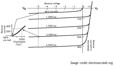
- Reverse Bias Region:
- In the reverse bias region, a reverse voltage is applied across the PIN photodiode.
- The reverse bias voltage extends the depletion region, enhancing the photodiode’s light absorption capability.
- As the reverse bias voltage increases, the depletion region widens, allowing for more efficient collection of photo-generated charge carriers.
- In this region, the photodiode acts as a current source, and the resulting current is the photocurrent generated by the incident light.
- The photocurrent is directly proportional to the intensity of the incident light.
- Photocurrent Saturation:
- In the reverse bias region, the photocurrent initially increases with increasing reverse bias voltage.
- However, there is a saturation point beyond which further increases in reverse bias voltage do not significantly affect the photocurrent.
- The saturation occurs when the depletion region encompasses the entire Intrinsic layer, and additional voltage does not contribute to further widening of the depletion region.
- Breakdown Region:
- If the reverse bias voltage continues to increase beyond the saturation point, the PIN photodiode may enter the breakdown region.
- In the breakdown region, the photodiode experiences a sharp increase in current, known as the breakdown current.
- This is an undesirable operating region for a photodiode as it can cause permanent damage and degrade the device’s performance.
Application of PIN photo diode
- Optical Communications:
- PIN photodiodes are widely used in optical communication systems, including fiber-optic communication networks.
- They serve as light detectors, converting optical signals into electrical signals for data transmission and reception.
- PIN photodiodes offer high responsivity, fast response times, and low noise characteristics, making them ideal for high-speed communication applications.
- Photovoltaic Power Generation:
- PIN photodiodes can be used as photovoltaic devices to convert light energy directly into electrical energy.
- They are utilized in solar cells and photovoltaic modules to generate electricity from sunlight.
- PIN photodiodes with high sensitivity to specific wavelengths can be tailored for efficient energy conversion in various solar cell designs.
- Environmental Sensing:
- PIN photodiodes are employed in environmental sensing applications, such as light level detection, ambient light sensing, and light intensity monitoring.
- They can be used in automatic brightness control (ABC) circuits for displays, ambient light sensors in smartphones and tablets, and light sensors in smart home automation systems.
- Imaging and Scanning:
- PIN photodiodes play a vital role in imaging applications, including digital cameras, surveillance systems, and medical imaging devices.
- They convert light signals into electrical signals, allowing for the capture and processing of images.
- PIN photodiode arrays are used for high-resolution imaging and scanning applications, such as barcode readers and document scanners.
- Scientific Research:
- PIN photodiodes are utilized in scientific research for light detection and measurement in various experiments and instruments.
- They can be employed in spectrometers, radiometers, and light meters for precise measurement of light intensity and spectral analysis.
- Industrial and Automotive Applications:
- PIN photodiodes find use in industrial applications such as laser alignment, industrial inspection, and quality control systems.
- They are also used in automotive applications, including optical sensors for proximity detection, rain sensing, and ambient light detection.
Advantages and disadvantages of pin photo diode
PIN photodiodes offer several advantages and disadvantages, which are important to consider when choosing them for a specific application. Here are the advantages and disadvantages of PIN photodiodes:
Advantages:
- High Sensitivity: PIN photodiodes have high sensitivity to light, allowing them to detect even low light levels accurately. They can capture weak optical signals effectively.
- Wide Spectral Response: PIN photodiodes have a wide spectral response range, enabling them to detect light across a broad range of wavelengths. This makes them suitable for applications that require detection of different wavelengths of light.
- Low Dark Current: PIN photodiodes typically have low dark current, which is the current flowing through the photodiode in the absence of light. Low dark current leads to higher signal-to-noise ratios and improved sensitivity.
- Fast Response Time: PIN photodiodes have fast response times, allowing them to quickly convert light signals into electrical signals. This makes them suitable for applications that require high-speed detection or modulation.
- Low Noise: PIN photodiodes exhibit low noise characteristics, leading to more accurate and reliable signal detection. Low noise allows for improved performance in applications where small signals need to be detected.
- High Quantum Efficiency: PIN photodiodes have high quantum efficiency, meaning they can efficiently convert incident photons into electrical current. This makes them suitable for applications where high sensitivity and efficient light conversion are critical.
Disadvantages:
- Large Size: PIN photodiodes tend to be larger in size compared to other photodetector types. This can limit their use in applications that require compact or miniaturized designs.
- Capacitance Effects: PIN photodiodes have inherent capacitance, which can cause a decrease in response time and limit their use in high-frequency applications.
- Temperature Dependence: The performance of PIN photodiodes can be influenced by temperature variations. Changes in temperature can affect the dark current and quantum efficiency of the photodiode.
- Power Consumption: PIN photodiodes require a reverse bias voltage to operate, which can consume power. This power consumption needs to be considered in low-power or battery-operated applications.
- Breakdown Voltage: PIN photodiodes have a maximum reverse bias voltage, beyond which they can enter the breakdown region and become damaged. Care should be taken to avoid exceeding the breakdown voltage during operation.
Read more wiki
What is a PIN photodiode?
A PIN photodiode is a type of photodetector that consists of three layers: P-type, Intrinsic (I) layer, and N-type. The Intrinsic layer is lightly doped, allowing it to have a larger depletion region for efficient light absorption.
How does a PIN photodiode work?
When photons (light) enter the depletion region of a reverse-biased PIN photodiode, they generate electron-hole pairs. These charge carriers are swept across the depletion region, resulting in a photocurrent. The magnitude of the photocurrent is proportional to the intensity of the incident light.
What are the advantages of using a PIN photodiode?
Some advantages of PIN photodiodes include high sensitivity to light, wide spectral response, low dark current, fast response times, low noise characteristics, and high quantum efficiency.
What are the applications of PIN photodiodes?
PIN photodiodes find applications in optical communications, photovoltaic power generation, environmental sensing, imaging and scanning devices, scientific research, industrial and automotive applications, and more.
Are PIN photodiodes temperature-sensitive?
Yes, PIN photodiodes can exhibit changes in their electrical characteristics with temperature variations. This can include shifts in dark current, responsivity, and quantum efficiency.
Can PIN photodiodes operate at high frequencies?
PIN photodiodes may have limitations in terms of their response time at high frequencies. The device’s capacitance and transit time of carriers can cause slower response to rapidly changing optical signals.